Stretchable alkenamides terminated Ti3C2Tx MXenes to release strain for lattice-stable mixed-halide perovskite solar cells with suppressed halide segregation
Abstract
Bandgap-tunable mixed-halide perovskite materials have attracted considerable interest because of their indispensability as top counterparts in tandem solar cells. However, the soft and disordered lattice always suffers from severe phase segregation under illumination, which is particularly susceptible to residual lattice strain. Herein, we report a strain regulation strategy by using alkenamides terminated Ti3C2Tx MXenes as an additive into perovskite precursor. Apart from the role of a template for grain growth to obtain high-quality films, the stretchable alkyl chain promotes lattice shrinkage or expansion to form an elastic grain boundary to eliminate the spatially distributed stain and shut down ion migration channels. As a result, the all-inorganic perovskite solar cells based on CsPbIBr2 and CsPbI2Br halides achieve prolonged device stability under harsh conditions and the best power conversion efficiencies up to 11.06% and 14.30%, respectively.
1 INTRODUCTION
During the past decade, the organic–inorganic hybrid perovskite solar cells (PSCs) are under the spotlight because of the unprecedented power conversion efficiency (PCE) of as high as 25.7% and continuous cost reduction by half of the commercial mono-Si solar cells.1-4 However, device stability is still a troublesome issue in further commercialization.5, 6 Different from the conventional semiconductors, for example, silicon or gallium arsenide, the soft ionic feature of perovskite materials inevitably induces the formation of lattice strain because of the incompatibility in ionic radii for an ideal crystal and thermal expansion coefficient between the substrate and the perovskite film during annealing and cooling processes,7, 8 which is regarded as an indispensable motive in downgrading the photovoltaic performances. More unfortunately, the detrimental strain effect is significantly amplified in accelerating phase segregation to generate I-rich and Br-rich domains under continuous illumination,9-11 when grafting onto the mixed-halide perovskite—one essential component as a top-cell in both perovskite/silicon and perovskite/perovskite tandem solar cells because of its easy bandgap tunability by regulating the I/Br ratio.12-14 As a result, the additional defects are formed to cause unwanted nonradiative recombination loss, slowing down the rapid propagation of mixed-halide wide-bandgap PSCs in comparison with monohalide perovskite tailored devices.15 Therefore, it is a prerequisite to release lattice strain and stabilize the mixed-halide perovskite lattice to achieve high-efficiency photovoltaics.16
Under persistent attacks by external stimuli, the perovskite lattices always suffer from tensile/compressive strain owing to the structural inhomogeneities, extruded grain boundaries, and lattice mismatch at the interface, which inevitably generates nonperiodic crystal lattice and accumulated defects at the buried interface and polycrystalline grain boundaries.7, 17, 18 By considering the vacancy-assisted ion migration mechanism,19 all the above scenarios will promote the phase segregation in these regions owing to the reduced energy barrier for ion migration and accelerated bandgap reduction, which are two main driven forces under tensile and compressive conditions.20, 21 It is well known that the confined lattice fluctuation including shrinkage or expansion determines the distortion degree in principle. Following this line of thought, the construction of an elastic grain boundary to avoid the strong confrontation between two adjacent interfaces/boundaries is logically practicable to release detrimental lattice strains.
To date, many strategies have been developed to achieve the above goal by adding various functional materials, mainly focusing on the organic small molecules or polymers,22, 23 which are easy to devitalize under high temperatures. As well known, MXene is a new two-dimensional (2D) carbon-containing inorganic compound with the general formula Mn+1XnTx, where M is a transition metal, X is a carbon or nitrogen atom, and Tx is a surface functional group,24 preliminarily demonstrating excellent advantages as an interface doping material for high-efficiency PSCs.25, 26 Compared to other 2D materials, the adjustable surface functional groups deliver more opportunities for tunning energy levels and passivation ability. Although MXene is beneficial for the film growth because of the interaction between end-capping functional groups (such as F, Cl, or OH) and perovskite surface,27, 28 the rigid heterostructure still localizes the lattice upon forming the one-off healing layer against the strain release under external temperature variation. In this work, we demonstrated a stretchable alkenamides terminated Ti3C2Tx MXene (SAM) as an additive to regulate the physicochemical characteristics of grain boundaries in inorganic mixed-halide perovskite films. The introduction of alkenamides to toughen the MXene surface not only passivates the under-coordinated Pb2+ defects based on Lewis acid–base chemistry but also frees the lattice movement to be like lattice “lubricant.” As a result, an elastic grain boundary can be formed through the above-mentioned precise control for obtaining a high-quality perovskite film with low defects, which in turn effectively suppresses the undesirable phase segregation and therefore improves the efficiency of wide-bandgap CsPbIBr2 and CsPbI2Br PSCs up to 11.06% and 14.30%, respectively. More importantly, the best device tailored with SAM remains 90% of initial PCE after 90 days of shelf-storage in dry air conditions and 70% after 100 h of persistent operation under one standard sun.
2 EXPERIMENTAL SECTION
2.1 Materials and reagents
Cesium iodide (CsI, 99.9%) and dimethylsulfoxide (DMSO, 99.7%) were purchased from Aladdin Chemistry Co., Ltd. Lead iodide (PbI2, ≥99.99%) was purchased from Xi'an Polymer Light Technology Corp. Lead bromide (PbBr2, 99.0%) was obtained from Macklin Reagent Co., Ltd. The low-temperature carbon paste (99.0%) was purchased from Shanghai MaterWin New Materials Co., Ltd. MAX materials (Ti3AlC2, 99.99%) were purchased from Mianyang Hengyang Electric Company. Lithium fluoride (LiF, 99.99%) was purchased from Sinonuo New Materials Technology Co., Ltd. Hydrochloric acid (HCl; AR) was purchased from Guangzhou Chemical Reagent Factory. All materials and reagents were acquired from commercial sources and used without further purification.
2.2 Fabrication of Ti3C2Tx MXene
1 g LiF was dissolved in 15 mL 9 M HCl, after which Ti3AlC2 powder was added and stirred in the above solution at 35°C for 48 h. At the end of the reaction, the suspension was centrifuged and washed several times with deionized water until the pH reached 6. The precipitated powder was collected by centrifugation and dried in a vacuum for later use.
2.3 Preparation of alkenamides terminated Ti3C2Tx MXene
1 g MXene and 1 g succinamide were mixed and dissolved in DMSO, and the mixutre was stirred for 24 h and then treated with ultrasound for 24 h, which was conducive to the stripping of MXene and the reaction with succinamide. The mixed solution (3500 rpm, 5 min) was centrifuged, and the supernatant was removed for later use.
2.4 Assembly of all-inorganic PSCs
Fluorine-doped tin oxide (FTO) glasses were firstly etched with HCl and Zn powder, and then completely washed with deionized water, isopropanol, and ethanol. Next, the cleaned FTO substrates were treated with plasma for 180 s before use. The compact TiO2 (c-TiO2) layer was fabricated by spin-coating an ethanol mixture of titanium isopropoxide (0.5 M) and diethanolamine (0.5 M) on FTO substrate at 7000 rpm for 30 s, followed by annealing at 500°C for 2 h. For CsPbIBr2 devices, the perovskite precursor solution was firstly constructed by fully dissolving CsI (260 mg, 1.0 mmol), PbBr2 (367 mg, 1.0 mmol), PbI2 (4.6 mg, 0.01 mmol), and 0.01 mg SAM in 1.0 mL DMSO. Then 90 μL of CsPbIBr2 perovskite precursor solution was spin-coated onto plasma-treated FTO/c-TiO2 surface at 1000 rpm for 10 s and 3000 rpm for 50 s. Next, the wet film was heated at 30°C for 1 min and then 260°C for 5 min. For CsPbI2Br devices, the perovskite precursor solution was established by thoroughly dissolved CsI (312 mg, 1.2 mmol), PbI2 (277 mg, 0.6 mmol), PbBr2 (220 mg, 0.6 mmol), and 0.01 mg SAM in 1.0 mL DMSO. The CsPbI2Br perovskite films were fabricated by spin-coating 90 µL of precursor solution onto plasma-treated FTO/c-TiO2 substrates at 500 rpm for 30 s and then at 3000 rpm for 40 s. After naturally cooling down, the carbon electrode was deposited with an active area of 0.09 cm2 by a doctor-blade coating method and heated at 70°C for 10 min.
2.5 Measurements and characterizations
The morphologies of as-prepared MXenes were obtained by transmission electron microscopy (TEM; Tecnai G2 F20) equipped with energy-dispersive spectroscopy (EDS). The atomic-force microscopy (AFM) image was obtained by AFM (Seiko SPA400). The morphologies of the prepared perovskite films were observed by scanning electron microscope (SEM; Hitachi S-4800). The detailed chemical states of as-prepared MXenes and perovskite films were estimated by X-ray photoelectron spectroscopy (XPS; Thermo ESCALAB 250XI). The crystal phase was determined utilizing X-ray diffraction (XRD) in a Bruker D8 Advanced diffractometer with a Cu Kα radiation source. Time-dependent ultraviolet–visible (UV–vis) absorption spectra were evaluated by means of a Meipuda UV-3200 spectrophotometer in the range of 400–700 nm under continuous illumination. Photoluminescence (PL) spectra were detected by using a Hitachi F-4500 fluorescence spectrophotometer with an excitation wavelength of 410 nm. To compare the phase segregation degrees for different films, WITec Alpha 300R confocal Raman microscopy was carried out to monitor the PL emission mappings. The time-resolved photoluminescence (TRPL) spectra were evaluated by the Delta Flex Fluorescence Lifetime System (Horiba Scientific Com.) excited by a 500 nm laser. Kelvin probe force microscopy (Cypher™; Asylum Research) was applied to determine the surface potential of the fabricated films. Photocurrent density–voltage (J–V) curves of PSCs were measured on an electrochemical workstation (CHI660E) under irradiation of simulated solar light (Newport, Oriel Class 3A, 91195A, AM1.5 G, 100 mW cm−2, calibrated by a standard silicon solar cell). External quantum efficiency (EQE) spectra were obtained using an IPCE kit from Enli Technology Co., Ltd. The light stability was performed under constant irradiation by a xenon lamp, and the error bar in the corresponding figure originated from the unstable light intensity. The Voc-decay curves were determined at open-circuit mode by illuminating for several seconds and then turning off the light. Capacitance–voltage (C–V) curves were recorded at a frequency of 5 kHz with an amplitude of 5 mV under dark at bias voltages from 0 to 1.80 V.
3 RESULTS AND DISCUSSION
MXene was fabricated by etching Al of Ti3AlC2 MAX-phase with HCl and LiF. As shown in Figure S1, accordion-like microstructure along with the evolution of XRD patterns demonstrates the transformation from a 3D phase to a 2D structure. After ultrasonic treatment, a colloidal dispersion with a green light beam is obtained in a DMSO solution (Figure S2), benefiting the application in PSCs. In the case of alkenamides terminated MXenes, tetra-carbonaceous succinimide is used to attach to the MXene surface via dehydration reaction in an acid bath, which will be discussed in the following part. Before the photovoltaic performance characterizations, we studied the fundamental properties of MXenes. As shown in Figure 1A,B, TEM images of MXenes with and without alkenamides termination both show 2D nanosheets with a size of 20 nm, demonstrating the negligible effect on morphology after alkenamides functionalization. However, the crystallinity is slightly weakened (the insets in Figures 1A,B and S3), which benefits in increasing the dispersibility owing to the reduced interlayer van der Waals force (Figure S2).29 To preliminarily confirm the successful commensality, we further performed the EDS mapping images of the SAM sample, as shown in Figures S4 and 1C–F; Ti, C, O, and N elements are clearly detected, comprehensibly assigning to the Ti3C2 MXene and alkenamides group.

XPS measurements of pristine and grafted MXenes were conducted to elucidate the intrinsic reaction mechanism between the terminal groups in MXene, such as –F, –Cl, and –OH with succinimide. Besides the typical four species including Ti–C, Ti(II)–Cl(F), Ti(III)–Cl(F), and TiO2 from Ti 2p spectra in Figure 1G, there is a new peak at a binding energy of 456.5 eV in SAM. It is an indicator of the formation of the Ti–O–C bond, which agrees well with the O 1 s spectra (Figure 1H).30, 31 Given the higher bond dissociation energies of Ti–F (569 kJ mol−1) and Ti–O (666.5 kJ mol−1) than that of Ti–Cl (405 kJ mol−1),30 the –OH and Ti–Cl groups are responsible for these substitution or elimination reactions because of the difficulty to perform postsynthetic covalent surface modifications of MXenes at Ti–F and Ti–O sites. Popular nucleophilic substitution and dehydration reaction will occur between MXene and succinimide by forming Ti–O− and –C═OH+ in H+-rich solution,31 respectively. In addition, the percentage of Ti–Cl is significantly reduced along with the increased intensity of the Ti–O peak upon the introduction of succinimide, suggesting the presence of halide ions exchange. Together with the detection of C═O and C–N signals in O 1s and C 1s spectra (Figures 1H,I and S5), we conclude that the organ-like MXene with an elastic surface is evidently fabricated (Figure 1J).
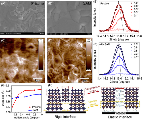
To study the impacts of stretchable MXene on perovskite film, we chose the Br-rich CsPbIBr2 as a pioneer owing to the more susceptible lattice to strain.21 Similar to previous reports,25 MXene also delivers an improved film quality with enlarged grain size (Figure 2A,B) and smoother surface (Figure S6) arising from the strong coupling interaction between functional groups and Pb atoms, which can be cross-checked by the Fourier-transform infrared spectroscopy measurement in Figure S7. Because of the small amount of additive in crystallized and intermediate phase perovskite films, it is difficult to explore the interaction between SAM and perovskite in depth. Therefore, we used PbBr2 and SAM mixture to better understand the mechanism behind the improved film quality. Compared to the pristine SAM, the characteristic vibration peaks from Ti–OH, C═O, C–N, and C–F are shifted and a new peak at ∼458 nm assigned to Pb–O is detected, demonstrating the strong electronic coupling interaction between termination groups in SAM and perovskite precursor. During the crystallization process, the nucleus generates around the additive, and the number of the nucleus is suppressed, implying retarded nucleation process and therefore slower crystal growth.32 After the transformation process, larger perovskite crystals could be obtained in the presence of SAM as an additive. No obvious change in characteristic diffraction peaks from XRD patterns and bandgap (Figure S8) demonstrates that MXenes mainly locate at the grain boundaries rather than are doped into the lattices. This phenomenon becomes more visible in the MXene-excess sample (Figure S9). As a result, the defective grain surface with trap density of 1–2 orders greater than that at the film interior is effectively healed to lower the overall defect density (Figure S10A),33 which in turn intensifies the PL probability and prolongs the carrier lifetime (Figure S10B,C). In addition to the improved film quality, another mechanism behind this comes from the donation of the lone electron pair on the terminal acylamino (such as –C═O and –NH2) to the under-coordinated Pb2+ based on the Pb 4f XPS spectra (a shift to lower binding energy in Figure S11),34 agreeing well with the higher surface potential (Figure 2C,D) because of the reduction of surface defects caused by dangling bonds.35 This can be further easily understood that more photogenerated holes will be accumulated on the perovskite surface with the structure of FTO/TiO2/perovskite owing to the suppressed nonradiative recombination.36

Different from traditional MXenes, the presence of flexible alkenamides with 4C chain is highlighted to give the freedom for lattice shrinkage or expansion to release residual strain. As shown in Figure 2E, the characteristic (100) reflection of the CsPbIBr2 phase gradually shifts to lower 2θ angles by increasing the X-ray incidence angle from 0.1° to 1.0°, meaning the increased planar spacing from 5.87 Å at the superficial layer to 5.90 Å at the buried surface; that is, the perovskite lattice suffers from spatially compressive-to-tensile strain conversion along the longitudinal depth. During the perovskite grain growth process at high temperatures, the CsPbIBr2 lattices inevitably anchor onto the underlying TiO2 surface, which hinders the perovskite lattice shrinkage. Because of the larger thermal expansion coefficient of CsPbIBr2 perovskite than that of the substrate, there will be a tensile lattice at the bottom surface in the cooling stage.37 Considering the typical perovskite film with a thickness of hundreds of nanometers, the properties of the top crystal lattice are believed to be different compared to that of the bottom surface. Arising from the lattice expansion and disordered crystal growth from precursor to cubic phase, the adjacent grains undergo pressure owing to the limited room for perovskite growth at the surface area, leading to the formation of in-plane compressive strain in perovskite films, which has been also reported previously.39, 38 After the incorporation of MXenes, this depth-dependent lattice spacing (or stain) is significantly eliminated (Figure 2F) and the corresponding values are summarized in Figure 2G. This trend is compatible with the (200) plane (Figure S12). Based on the above results, SAM with a long alkyl chain can provide an elastic interface to compensate for the thermal expansion mismatch between perovskite and TiO2 layers and buffer intergranular extrusion (Figure 2H), leading to the strain-less perovskite film.40 To cross-check this, we further characterized the crystal lattice evolution of superficial perovskite surface by characterizing the scanning transmission electron microscope images owing to the difficulty to explore the buried interface. As shown in Figure S13, obvious lattice distortion is detected in pristine film, and the lattice spacing is increased after the incorporation of SAM, displaying significantly improved crystallization. In addition, we also explored the tendency of lattice strain with component binding energy. From the high-resolution XPS spectra of Cs 3d, Pb 4f, I 3d, and Br 3d, as shown in Figure S11, a slight shift of Pb, Br, and I peak positions to lower binding energies is observed upon releasing the compressive strain on the surface area, while the binding energies of Cs 3d exhibit little variations. The behind mechanism can be attributed to the lattice enlargement and redistributed electron density. Following this line of thought, the electronic properties of halide perovskites, which is highly dependent on the adjacent electronic overlap of corner-shared [PbX6]4− octahedra, are well regulated. As for the buried interface, by releasing the tensible strain, an increase in charge transport of perovskite material could be obtained owing to the enhanced overlap of the atomic orbitals,41 leading to the preferable charge transfer. As for the top surface, although the valence band maximum is shifted upward because of the stronger orbital overlapping between Pb 6s and I/Br 5p orbitals under compressive lattice,42 the significantly reduced defects will play a more important role in improving the photovoltaic performance of PSCs.39
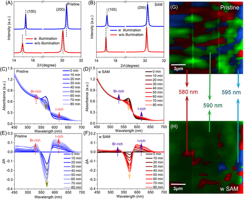
As one crucial bottleneck in determining the application of mixed-halide PSC, the detrimental phase segregation is minimized because of the high dependence on the defective lattice. We first investigated the evolution of XRD patterns of perovskite films after persistent light irradiation. As shown in Figure 3A,B, both films show a diffraction peak shift to a larger angle, demonstrating the formation of the Br-rich phase (I-rich phase prefers to decompose into the yellow phase, as illustrated in Figure S14). After close observation, this scenario is weakened for SAM-tailored film by reason of the released strain and reduced defect. To understand more details under light irradiation, we monitored the time-dependent UV–vis absorption spectral evolution (Figure 3C,D) and calculated the corresponding absorption difference (ΔA) (Figure 3E,F). Strikingly, three fingerprint regions are observed, including gradual absorption degradation at windows of 545–585 nm (ΔA < 0) and enhancement at windows of 585–660 nm (I-rich domains)/450–545 nm (Br-rich domains) (ΔA > 0) with two approximately invariant wavelengths at 545 and 585 nm by prolonging the exposed illumination time to 80 min, clearly suggesting that the demixing conversion takes place with quasi-equilibrium model (similar shape of ΔA).43 In addition, hyperspectral PL mapping images with different spectral windows, that is, at 580, 590, and 595 nm marked in red, green, and blue colors, respectively, are characterized to intuitively display the inhomogenous phase distribution on the perovskite surface. As shown in Figure 3G, the pristine film suffers from multicolored emission peaks, undoubtedly ascribing to the phase segregation-induced component deviation. On the contrary, a much more homogeneous PL feature with significantly reduced red and blue areas is observed by bringing in stretchable SAM (Figure 3H), again cross-checking the positive effect of this concept-of-physical elastic interface to heal the defective lattice and thereby shut down the ion migration channels.

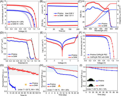
Finally, we fabricated the mixed-halide CsPbIBr2 PSCs with a structure of FTO/c-TiO2/CsPbIBr2/carbon (Figure S15) to study the impacts of SAM on photovoltaic performances. From the characteristic current J–V curves in Figures 4A, S16, and S17, the strain-released device exhibits a champion PCE up to 11.06% with open-circuit voltage (Voc) of 1.317 V, short-circuit current density (Jsc) of 11.81 mA cm−2, and fill factor of 71.10%, which is much higher than 7.48% for the control one as well as 10.50% for the pristine MXene tailored PSC, along with reduced hysteresis index from 29% to 20%, which is in accordance with the results from steady power outputs (10.84% vs. 6.86% in Figure 4B) and EQE spectra (10.90 vs. 8.12 mA cm−2 in Figure 4C). Undoubtedly, the performance enhancement is caused by the stabilized crystal lattice and reduced defects. Mott–Schottky measurement was employed to calculate the built-in electric field (Vbi). As shown in Figure 4D, the Vbi of pristine and optimal PSCs are 1.31 and 1.60 V, respectively, demonstrating the increased driven force for charge extraction and transfer, which is consistent with the Voc increase. In this fashion, the photogenerated electrons can survive longer at the conduction band of perovskite film with a slower voltage decay rate upon removing the light irradiation (Figure S18). As a result, by recording the dark J–V curves shown in Figure 4E, the champion PSC displays a smaller leakage current than the control PSC, which is attributed to the suppressed nonradiative recombination loss (Figure S19). This efficiency advancement also works well in CsPbI2Br PSC with a champion PCE of 14.30% (Figures 4F and S20), demonstrating its universal applicability to SAM-induced elastic interface. After persistent operation over 100 h under AM1.5G sunlight illumination (Figure 4G), dark storage over 22 and 90 days in high temperature (T = 85°C) and dry air (relative humidity, RH = 10%) conditions (Figures 4H,I, S21, and S22), the best PSC remains as the higher PCE conservation rate compared to the untreated device.

4 CONCLUSION
In summary, we demonstrated an elastic grain boundary to universally release the lattice strain and passivate the defects by incorporating stretchable Ti3C2Tx MXene into perovskite films. Arising from the stabilized lattices or grain boundaries, the overall PCEs of all-inorganic CsPbIBr2 and CsPbI2Br PSCs are significantly improved up to 11.06% and 14.30% with excellent long-term durability in harsh conditions, respectively. As is well known, 2D materials show great potential in promoting the efficiency and stability of PSC. However, the current research studies are mainly focused on the effect of 2D materials on perovskite film. The detailed functional manipulation of 2D materials and their application in PSC are lacking, such as the optimization of species and alkyl chain length of terminated groups located on the 2D material surface. By tuning the properties of 2D materials, high-quality perovskite films with reduced defect and released strain can be obtained in the future. These results show the great potential in promoting the feasible usage of wide-bandgap-based PSCs in tandem cells.
ACKNOWLEDGMENTS
The authors gratefully acknowledged financial support provided by the National Natural Science Foundation of China (Grant Nos. 22109053, 22179051, 62104136), Special Fund of Taishan Scholar Program of Shandong Province (tsqnz20221141), National Key Research and Development Program of China (2021YFE0111000), Spring City Plan: the High-level Talent Promotion and Training Project of Kunming (2022SCP005), the Guangdong Basic and Applied Basic Research Foundation (2020A1515110548), and the Guangzhou Science and Technology Planning Project (202102020775, 202102010091).
CONFLICT OF INTEREST STATEMENT
The authors declare no conflicts of interest.


