Multifunctional Buffer Layer Engineering for Efficient and Stable Wide-Bandgap Perovskite and Perovskite/Silicon Tandem Solar Cells
Graphical Abstract
A facile strategy incorporating AlOx deposited by controlled growth was developed to modulate the perovskite surface. The infiltrated Al3+ can suppress ion migration and phase separation, regulate the arrangement of energy levels, and passivate defects on the perovskite surface and grain boundaries. A monolithic perovskite-silicon tandem solar cell achieved a PCE of 28.50 % with excellent photothermal stability.
Abstract
Inverted perovskite solar cells (PSCs) are preferred for tandem applications due to their superior compatibility with diverse bottom solar cells. However, the solution processing and low formation energy of perovskites inevitably lead to numerous defects at both the bulk and interfaces. We report a facile and effective strategy for precisely modulating the perovskite by incorporating AlOx deposited by atomic layer deposition (ALD) on the top interface. We find that Al3+ can not only infiltrate the bulk phase and interact with halide ions to suppress ion migration and phase separation but also regulate the arrangement of energy levels and passivate defects on the perovskite surface and grain boundaries. Additionally, ALD-AlOx exhibits an encapsulation effect through a dense interlayer. Consequently, the ALD-AlOx treatment can significantly improve the power conversion efficiency (PCE) to 21.80 % for 1.66 electron volt (eV) PSCs. A monolithic perovskite-silicon TSCs using AlOx-modified perovskite achieved a PCE of 28.5 % with excellent photothermal stability. More importantly, the resulting 1.55 eV PSC and module achieved a PCE of 25.08 % (0.04 cm2) and 21.01 % (aperture area of 15.5 cm2), respectively. Our study provides an effective way to efficient and stable wide-band gap perovskite for perovskite-silicon TSCs and paves the way for large-area inverted PSCs.
Introduction
Multi-junction tandem solar cells (TSCs) have garnered research attention for their competitive advantages in overcoming the Shockley–Queisser efficiency limitations of single-junction solar cells.1-3 Perovskite solar cells (PSCs) have tunable band gaps, long charge carrier diffusion lengths, superior light collection efficiency, and facile fabrication processes, contributing to their impressive efficiency rate of 26.1 %.4, 5 These qualities make PSCs ideal candidates for top cells in TSCs.6 The certified efficiency of perovskite-on-silicon 2-terminal TSCs stands at 33.9 %.7 However, the issue of light-induced phase segregation (LIPS) in wide-band gap (>1.65 electron volts, eV) iodide/bromide (I/Br) mixed perovskite absorbers poses a challenge to the power conversion efficiency (PCE) and stability of perovskite-based TSCs.8-10 Substantial efforts have been dedicated to mitigating halide segregation through crystallization control, defect passivation, and strain engineering methods.11-14 Despite some encouraging progress, the photostability of wide-band gap PSCs remains unsatisfactory.15
Moreover, the solution processing and the low formation energy of perovskites inevitably lead to numerous defects formed at both the bulk and interfaces of the perovskite layer.16-18 These defects can act as non-radiative recombination centers, significantly impeding carrier transport.19-21 This ultimately results in a substantial deficit in the open-circuit voltage (Voc), particularly at the interface between perovskites and fullerene electron transport layers (ETLs) in inverted PSCs.22, 23 Passivating these defects is paramount in realizing the high efficiency and stability of PSCs.24 Various strategies have been devised to tackle these challenges, including composition tuning, employing low-dimensional perovskites, and optimizing interfaces.25-27 However, many of these approaches rely on the spin-coating method, which is unsuitable for treatment on textured surfaces and may not be compatible with large-area substrates.
Atomic layer deposition (ALD) has found widespread application as a highly effective method for depositing large-area thin films.28 It has been utilized in fields ranging from organic light-emitting diodes (OLEDs) to silicon and thin-film solar cells.29, 30 When applied between the surface of the perovskite layer and the transport layer, AlOx deposited via ALD has proven to be efficacious in enhancing the performance of PSCs.30, 31 While most studies focus on methylammonium (MA)-based perovskites,32 the working mechanism and functions of these AlOx layers remain unclear, particularly for formamidinium (FA)-based perovskites.
Here, a facile and efficient strategy is employed for precisely modulating the perovskite by incorporating AlOx deposited by ALD on the top interface. Al3+ ions were found to be infiltrated in the perovskite layer and interact with halide ions. The treatment contributed to realizing better-matched energy levels, suppressed ion migration and minimized interfacial carrier losses simultaneously. Additionally, the self-encapsulation effect of this dense interlayer can inhibit volatile ion overflow at high temperatures and improve light and thermal stability. Consequently, the ALD-AlOx modification could significantly improve the PCE of wide-band gap PSCs from 19.32 % to 21.80 % and enhance their photothermal stability. More importantly, a monolithic perovskite-silicon TSC using AlOx-modified perovskite achieved a PCE of 28.50 % with good stability. The resulting 1.55 eV PSC and module also achieved a PCE of 25.08 % (0.04 cm2) and 21.01 % (aperture area of 15.5 cm2), respectively, proving the universality of the strategy.
Results and Discussion
The ultrathin AlOx film was fabricated by atomic layer deposition (ALD) with trimethylaluminum (TMA) and H2O. As shown in Figure 1, TMA and H2O are alternately exposed to a substrate in a repeated TMA-pulse-purge-H2O-pulse-purge sequence, and we proposed a growth mechanism of ALD AlOx on top of perovskite (Figure 1).32, 33 During the first half-cycle (equation 1), TMA reacts with the perovskite surface by interacting with the organic cation (MA+ or FA+), which weakens the hydrogen bonds between the organic cation and I− of the perovskite, leading to a breakdown of the perovskite framework on the surface. The adduct comprising of X3Pb-Al(CH3)-PbX3 as the key intermediates was generated accompanied by the release of CH4 and FA or MA, and then, X3Pb-Al(CH3)-PbX3 reacted with the H2O molecule during the subsequent half-cycle and produced the −OH surface sites (X3Pb-Al(OH)-PbX3) (equation 2), which are considered to be the most ubiquitous chemisorption sites for TMA and necessary to promote the growth of AlOx. With the increased number of ALD cycles (equations 3 and 4), a dense AlOx film was formed on the perovskite. The final thickness of AlOx can be precisely controlled by the number of ALD cycles.
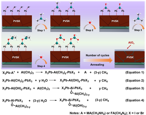
The schematic of the proposed growth mechanism of ALD-AlOx on top of perovskite and the proposed reaction mechanism between TMA and perovskite.
We verified the ultrathin nature of the AlOx interlayer with high-resolution scanning transmission electron microscopy (HR-STEM). As shown in Figure 2a and S1, the STEM images and energy-dispersive X-ray spectroscopy (EDS) mapping clearly outline the perovskite/AlOx/C60/SnO2 top contact structure, identifying the presence of a ~18 nm C60 layer and a ~10 nm SnO2 layer. Interestingly, Al3+ ions are found to be diffused to the bulk and throughout the whole perovskite layer (Figure S2), which are supposed to exist in the grain boundaries rather than dope within the perovskite lattice due to the much smaller ionic radius than Pb2+ (53.5 pm vs. 119 pm).34, 35 There is no noticeable change in the X-ray diffraction (XRD) of the perovskite film before and after modifying with ALD AlOx (Figure S4), confirming our speculation. In addition, the modified perovskite films in atomic force microscope (AFM) and scanning electron microscopy (SEM) exhibited reduced roughness and increased grain size, indicating that the surface morphology was improved by AlOx treatment (Figure S5–S6). The infiltrated Al3+ ions at the grain boundaries and perovskite surface would passivate the antisite PbX3− (X means I or Br) defects and suppress the ion migration pathway, facilitating the phase stability of bromine-rich wide-band gap perovskite. Moreover, the dense interlayer of AlOx not only acts as an inner encapsulation but also regulates the energy level arrangement at the perovskite/C60 interface (Figure 2b).
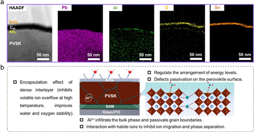
(a) High-angle annular dark-field (HAADF) image in HR-STEM and the corresponding EDS mapping at the electron-transporting layer side. (b) Schematic diagram of the function and mechanism of ALD-AlOx in the device.
The energy band structure of perovskite (PVSK) and PVSK/AlOx was determined via ultraviolet photoelectron spectroscopy (UPS) and optical band gap (Eg) values. As shown in Figure 3a and Figure S7, the Fermi levels (EF) of PVSK film are calculated from the equation of EF=h −Ecut-off (h =21.2 eV), which upshifts from −4.27 to −4.19 eV after capping with AlOx. The conduction band minima (CBM) of the PVSK/AlOx is evaluated by the valence band maxima (VBM) and Eg values, which is determined to be −4.09 eV, bringing it closer to the CBM of C60 than PVSK (−4.10 eV). Kelvin probe force microscopy (KPFM) was carried out to explore their surface potentials, as shown in Figure 3b–c and S7. The surface of PVSK/AlOx exhibits an average surface potential of 787 mV, which is higher than that of bare PVSK film (557 mV), consistent with the results of the UPS measurements above. The lower offset between EF and CBM of PVSK/AlOx indicates its stronger n-type characteristics, which could suppress the trap-assisted recombination loss and promote charge extraction from perovskite to ETL efficiently, resulting in an improved Voc.36, 37
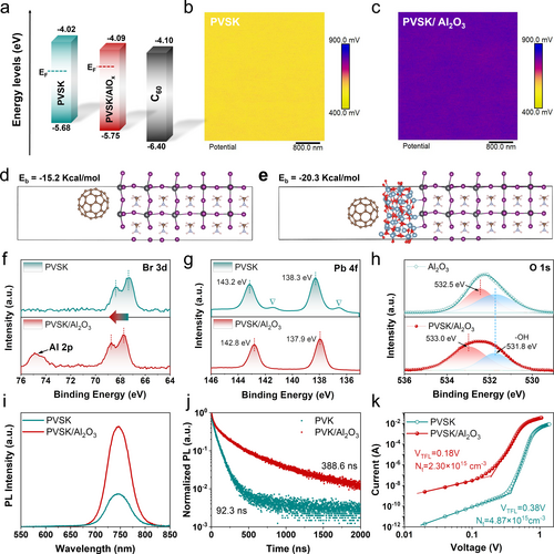
(a) The schematic diagram of the energy level arrangement of the pristine PVSK, PVSK/AlOx and C60 in the devices. (b–c) The KPFM images of (b) pristine PVSK and (c) PVSK/AlOx films. (e–f) The calculated binding energy of (e) PVSK/C60 and (f) PVSK/AlOx. (f–h) XPS spectra of (f) Br 3d and (g) Pb 4f pristine PVSK and PVSK/AlOx films. (h) XPS spectra of O 1s for bare AlOx and PVSK/AlOx films. (i) The photoluminescence (PL) and (j) time-resolved photoluminescence (TRPL) spectra of the pristine PVSK and PVSK/AlOx films. (k) Different I−V curves of electron-only devices based on pristine PVSK and PVSK/AlOx in the dark.
To unravel the mechanism behind the impact of the AlOx interlayer, we conducted DFT calculations to explore the interaction between C60 and the perovskite surface. As depicted in Figure 3d–e, the C60 and PVSK/AlOx surface exhibits higher binding energy −20.3 kcal mol−1 than that of C60 and PVSK (−15.2 kcal mol−1). The larger binding energy suggests tighter packing between C60 and PVSK/AlOx, improving the interfacial contact between perovskite and C6038 and contributing to the enhanced thermal stability of the device (discussed below). Moreover, a surface dipole can increase the local work function and hinder efficient electron extraction.39 The z-component of the dipole moment (Dz) is calculated to be maximal for the PVSK/C60 system (4.10 Debye) and is reduced to 2.31 Debye after the insertion of AlOx interlayer (Figure S9), consistent with the trend of work functions measured by UPS.40
X-ray photoelectron spectroscopy (XPS) was provided to further insight into the chemical modification of the perovskite. As shown in Figure 3f, the presence of AlOx is verified by the additional Al 2p peak at 74.8 eV for PVSK/AlOx.41 The Br 3d spectrum of PVSK/AlOx slightly shifted to higher binding energies, which could be a result of the electron transfer between the Al3+ ion and Br− in perovskite.35 Furthermore, both Pb 4f7/2 and Pb 4f5/2 peaks (Figure 3g) shift towards lower binding energy values by 0.4 eV after the AlOx modification, which is attributed to the passivation of Pb-rich surface defects with lattice oxygen of AlOx. Moreover, the two weak signals of Pb 4f7/2 at ∼136.5 eV and Pb 4f5/2 at ∼141.4 eV in the pristine PVSK correspond to the metallic Pb0 (Figure 3g), which disappear after the capping with AlOx, indicating that AlOx significantly suppresses the formation of metallic Pb0 on the perovskite surface.42 The O 1s of bare AlOx can be de-convoluted into the Al−O bond at 532.5 eV and −OH bond at 531.8 eV43 (Figure 3h), and the characteristic peaks of Al−O shift towards higher binding energy from 532.5 eV to 533.0 eV, which further confirmed the interaction between AlOx and perovskite. The interaction was also demonstrated by the peak shifts of I 3d in the perovskite film before and after AlOx treatment (Figure S10).
where VTFL represents the transition voltage between ohmic and trap-filling regions, e is the elemental charge, and L is the perovskite film thickness. As determined from the density–voltage (J−V) curve of the electron-only devices in the dark (Figure 3k), the corresponding trap densities (Nt) were determined to be 4.87×10¹⁵ and 2.30×1015 cm−3 for the devices based on PVSK and PVSK/AlOx, respectively. The reduced Nt of the perovskite film capping with AlOx is ascribed to its passivation capability on the perovskite surface and grain boundaries,48 consistent with the analysis of XPS mentioned above.
The single-junction wide-band gap perovskite solar cells were first fabricated with and without the AlOx layer. The device configuration is ITO/MeO-2PACz/Perovskite/AlOx/C60/SnO2/Ag (Figure 4a), and the J−V curves were measured under one-sun illumination. The optimized J−V curves and data of control and target PSCs are shown in Figure 4b and Table S3. The devices incorporating AlOx showed the highest PCE of 21.80 % with a short-circuit current density (Jsc) of 22.59 mA cm−2, Voc of 1.181 V, and fill factor (FF) of 81.72 %. By contrast, the control cell presented a much lower PCE of 19.32 % due to the lower Voc of 1.126 V and FF of 78.62 % (Figure S12). The integrated Jsc derived from external quantum efficiency (EQE) spectra (Figure 4c) are 21.26 and 22.00 mA cm−2 for the control and target device, respectively, approximate to their measured Jsc. The steady-state power output (SPO) at the maximum power point was carried out to verify the performance of modified PSCs (Figure S13–S14). The PCE of the optimized device was further verified by the stabilized power output measurements at the maximum power point (Vmax=1.00 V for target, Vmax=0.96 V for control) for 200 s, which shows a stabilized PCE of 21.23 % and 18.53 % for the target and control device, respectively. Moreover, the target cells exhibit good reproducibility with an average PCE of 21.17 % (Figure 4d), much better than the control device (19.40 %). The improved performance of the target cell with the AlOx layer mainly originated from the increased FF and Voc (Figure S15). Accordingly, the built-in potential (Vbi) of the devices is derived from the capacitance-voltage curves, which were characterized to directly compare by the Mott–Schottky analysis.49 The target device with an AlOx layer exhibits a larger Vbi of 1.07 V than that of the control cell (1.05 V) (Figure 4e), indicating a stronger driving force of the target device for separating photogenerated charge carriers, which is facilitated to achieve a higher Voc. We ascribe the superior Vbi to the better-matched energy level alignment and defect passivation at the perovskite/ETL interface. Moreover, the leakage currents from the dark J−V curves of PSCs were performed (Figure 4f). The reverse leakage current and ideal factor (m) of the target device with the AlOx layer is smaller than that of the control, indicating the minimized shallow defect states and trap-assisted Shockley–Read–Hall recombination.50 The results are in accordance with the measurements of electrochemical impedance spectroscopy. The Nyquist plots for different PSCs with and without the AlOx layer were measured at 1.0 V, ranging from 106 to 1 Hz in the dark. As shown in Figure 4g, the charge transport resistance of the target device (934 Ω) was much lower than that of the control cell (1692 Ω), further confirming the adequately suppressed carrier recombination at the perovskite/C60 interface or in bulk.
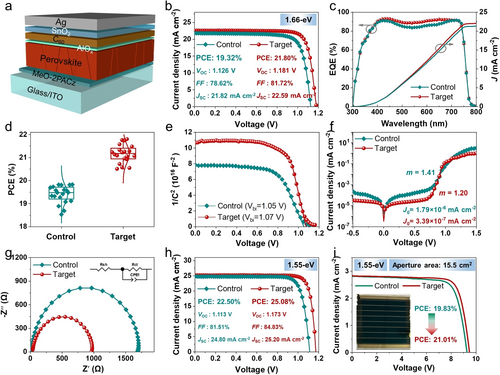
(a) The configuration of single-junction wide-band gap PSCs. (b) Optimized J−V curves of control and target device. (c) The EQE spectra with the integrated Jsc of the control and target PSCs. (d) PCE distribution of 20 devices based on control and target PSCs. (e) Mott–Schottky plots of the corresponding PSCs. (f) Dark J−V curves of the control and target devices. (g) Nyquist plots of PSCs with and without AlOx layer measured at 1.0 V in the dark ranging from 106 to 1 Hz. (h) The optimized J−V curves of inverted PSCs with 1.55 eV. (i) The J–V curves of its corresponding mini-modules with an aperture area of 15.5 cm2.
To investigate the universality of our strategy in enhancing inverted device performance, we have also extended the application of the AlOx treatment to the devices utilizing perovskite absorber materials with band gaps of 1.55 eV. The detailed device fabrication process of the optimized PSCs is presented in the Supporting Information. As shown in Figure 4h, the optimized device based on the AlOx modification yields an efficiency of 25.08 % with a high Voc of 1.173 V, an FF of 84.83 % and a Jsc of 25.20 mA cm−2. Additionally, we successfully fabricated a PSC mini-module with an aperture area of around 15.5 cm2 (The geometric fill factor is 92.4 %) and tested its J–V characteristics (Figure 4i). The PCE of the mini-module with 8 sub-cells reached 21.01 %, with a Voc of 9.474 V, a Jsc of 2.833 mA cm−2 and an FF of 78.27 %.
The stability of perovskite-based TSCs is largely dependent on wide-band gap perovskites. Therefore, we performed in situ photoluminescence (in situ PL) to evaluate the stability of wide-band gap perovskites under light illumination conditions. As shown in Figure 5a, b and S15, the PL peak of the control film was significantly redshifted after continuous illumination (laser) for 150 seconds. Simultaneously, a new PL peak with lower photon energy (~1.59 eV), indicative of halide segregation, gradually appeared in the PL spectrum of the control sample within 150 seconds. Furthermore, the increase in the full width at half maximum (FWHM) (Figure 5d) and the reduction in PL intensity (Figure 5c) indicated the formation of new iodine-rich and bromine-rich phases.51 In contrast, the target film showed consistent PL peak positions, PL intensity, and FWHM values, suggesting that the infiltrated Al3+ effectively impedes ion migration pathways and maintains the structural stability of the perovskite crystal. The long-term stability of wide-band gap PSCs was further explored. As depicted in Figure 5e, the target PSC can sustain over 97 % of its initial PCE after being stored in N2 for 3500 hours. In comparison, the PCE of the control one dropped to 54 % of the initial value. The moisture and oxygen stability of the PSCs were conducted under a relative humidity (RH) of 35±5% (Figure S17). The target PSC maintains approximately 90 % of its original PCE after storing over 1300 hours. In contrast, the control PSC declines to 43 % of its original PCE. Moreover, we further investigated the light stability under continuous light soaking (white LED, 100 mW cm−2) in a glove box. The target PSCs with the AlOx layer can maintain over 87 % of their original PCE after 1560 hours, while the PSC based on pristine PVSK dropped to 57 % of its premier value (Figure 5f). We explored the thermal aging test under one-sun irradiation to accelerate the aging test. As shown in Figure 5g, the unencapsulated device modified by the AlOx layer could sustain 78 % of its original PCE after being stored at 65 °C in N2 under continued light soaking for 672 hours, while the PCE of the control cell retained only 38 % of its initial value. The thermal stability of the perovskite films was also tracked using XRD measurements. As shown in Figure 5h and 5i, the diffraction peak around 12.3° is assigned to the characteristic peak of PbI2, which was observed for the pristine perovskite film after 10 days. The diffraction intensity sharply decreases along with the storage time due to the phase segregation of wide-band gap perovskite. In contrast, no obvious PbI2 signals existed until 25 days. These results proved that the multifunctional buffer layer engineering of AlOx promoted the higher phase stability of wide-band gap perovskite films. The enhanced performance and stability of the wide-band gap PSCs based on the AlOx layer should be responsible for the improved intrinsic stability of the perovskite film and restrained defect density at the perovskite/C60 interface and perovskite grain boundary.
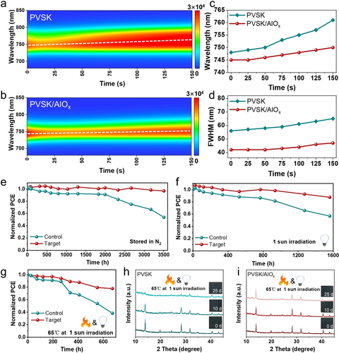
The in situ photoluminescence of wide-band gap perovskite film for (a) control and (b) target samples. (c) The PL peak positions and (d) the extracted full width at half maximum (FWHM) of the control and target perovskite films with various illumination times. (e) PCE evolution of the unencapsulated wide-band gap PSCs with and without AlOx layer stored in N2. (f) PCE evolution of the unencapsulated wide-band gap PSCs with and without AlOx layer stored in N2 under continuous irradiation (1 sun illumination, white light-emitting diode (LED), 100 mW cm−2). (g) PCE evolution of the unencapsulated wide-band gap PSCs with and without AlOx stored in the glove box at 65 °C under continuous irradiation (1 sun illumination, white LED, 100 mW cm−2). (h) The XRD patterns of the wide-band gap perovskite film with and without the AlOx layer stored in the glove box at 65 °C under continuous irradiation (1 sun illumination, white LED, 100 mW cm−2).
Furthermore, we fabricated two-terminal perovskite/silicon heterojunction TSCs using the modified perovskite to validate the applicability of the AlOx layer in the perovskite/silicon TSCs. Figure 6a shows the device schematics of TSCs in this work, and the cross-section SEM image is shown in Figure S18. As shown in Figure 6b and S18, the best TSC after AlOx modification exhibits a champion PCE of 28.50 % with a Jsc of 20.64 mA cm−2, a Voc of 1.819 V, and an FF of 75.92 %. The integrated Jsc from EQE spectra of the optimized tandem cell is 20.36 and 19.90 mA cm−2 for the top and bottom sub-cells (Figure S20), respectively, which is within the accuracy confidence of the measurements. Detailed photovoltaic parameters are summarized in Table S4. Also, maximum power point tracking of the target TSC demonstrates stable power outputs with a stabilized PCE of 28.05 %, and there is no distinctive performance drop over 600 s (Figure 6c). The TSCs show good reproducibility with an average efficiency of 27.87 %, much better than the control devices (25.11 %). (Figure 6d and Figure S21). Moreover, the TSCs cooperating with the AlOx layer show excellent light and thermal and moisture stability. As shown in Figure S22, the target TSCs sustain over 90 % of their initial PCEs over 800 hours under one-sun light soaking, continuous heating at 65 °C or relative humidity (RH) of 35±5%, respectively. The excellent efficiency and stability can be attributed to the higher intrinsic stability of AlOx-based wide-band gap perovskite, suggesting the potential of the AlOx layer for high-performance TSCs.

(a) Device schematics of textured 2-terminal perovskite/silicon TSCs studied in this work. (b) J−V curves of control and target champion TSC devices under reverse scan. (c) The steady-state power output of the champion target TSC device. (d) The distribution of the photovoltaic characteristics of 20 devices for the control and target TSCs.
Conclusion
This work demonstrates a facile and effective strategy for precisely modulating the perovskite by incorporating AlOx deposited by ALD on the top interface. Al3+ can not only infiltrate the bulk phase and interact with halide ions to suppress ion migration and phase separation, but also regulate the arrangement of energy levels and passivate defects on the perovskite surface and grain boundaries. Consequently, the ALD-AlOx treatment can significantly improve the PCE to 21.80 % for wide band gap PSCs and 28.50 % for monolithic perovskite-silicon TSCs. More importantly, ALD-AlOx exhibits a self-encapsulation effect through a dense interlayer, significantly improving the photothermal stability of PSCs. In addition, the resulting 1.55 eV PSC and module also achieved a PCE of 25.08 % (0.04 cm2) and 21.01 % (aperture area of 15.5 cm2), respectively, proving the universality of the strategy.
Acknowledgments
X. J., Y. D. and L. B. contributed equally to this work. L. L. is grateful for the financial support from Shanxi Province Science and Technology Department (20201101012, 202101060301016). A. K. Y. J. thanks the sponsorship of the Lee Shau-Kee Chair Professor (Materials Science), and the support from the APRC Grants (9380086, 9610419, 9610440, 9610492, 9610508) of the City University of Hong Kong, the TCFS Grant (GHP/018/20SZ) and MRP Grant (MRP/040/21X) from the Innovation and Technology Commission of Hong Kong, the Green Tech Fund (202020164) from the Environment and Ecology Bureau of Hong Kong, the GRF grants (11307621, 11316422) and CRS grants (CRS_CityU104/23, CRS_HKUST203/23) from the Research Grants Council of Hong Kong, the Shenzhen Science and Technology Program (SGDX20201103095412040), Guangzhou Huangpu Technology Bureau (2022GH02), and the Guangdong Major Project of Basic and Applied Basic Research (2019B030302007).
Conflict of interests
The authors declare no conflict of interest.
Open Research
Data Availability Statement
The data that support the findings of this study are available from the corresponding author upon reasonable request.


