Free-space Optical Computing Systems
Abstract
Free-space optical systems are emerging as a hardware platform for high-throughput and energy-efficient computing. In this review, the pioneering works are first introduced to lay the foundation for the principles and architectures of systems. The modern hardware implementations of two types of optical computing systems, matrix, and vector multiplication systems and diffractive optical neural network systems, are covered from material, device, and system perspectives. Further, the system deployment to various applications is also discussed. This review serves as an introduction and guideline to the current progress of developing and utilizing free-space optical computing systems in various domains.
1 Introduction
High-performance computing hardware has been a backbone for scientific and technological advancement and backthroughs. In particular, the past decade has witnessed an unprecedented performance of machine learning (ML) algorithms in a broad range of application domains, such as imaging science and technology,[1-3] material informatics,[4, 5] and electronic chip design.[6] However, the current electronic computing hardware has started to hit a bottleneck of further reducing energy consumption and simultaneously increasing the integration density to catch up with the explosively increasing scale of needed computing resources and energy,[7, 8] thus calling for emerging high-throughput and energy-efficient hardware platforms. Recently, optical systems have attracted much interest as computing hardware by leveraging photons, which are fundamentally different particles from electrons, to break down the electronic bottleneck thanks to their intrinsic fundamental properties, such as the high parallelism from the weak photon–photon interaction, high-capacity multiplexing, and ultralow static energy consumption.[9]
Although various integrated 2D optical circuits have been demonstrated for computing thanks to the advance of semiconductor manufacturing,[10-14] these circuits have a fundamental limitation on the achievable scalability because of the co-planar layout of information processing (e.g., modulators) and routing components (e.g., waveguides). In contrast, 3D free-space optical systems perform mathematical calculations based on two fundamental operations on optical wavefronts: 1) spatial manipulation and 2) free-space propagation. Hence, their computing units for spatial manipulation are in a 2D plane, such as using spatial light modulators (SLMs), while the light routing is along the direction orthogonal to the 2D plane. This decoupling scheme can enable the scale of millions of computing components with mature device technologies and single-clock-cycle computing in one light pass-through.
This review will be organized as follows. In Section 2, we will first review early pioneering works on 3D optical computing systems. Although the electronic and optical hardware then limited the demonstration scale and application space of these systems, the developed fundamental principles have laid solid foundations. In Section 3, we will review one category of optical computing systems – optical matrix and vector multiplication systems. We will first discuss the implementation of modern systems using state-of-the-art components. Further, we will mention some novel materials and devices, which can be incorporated into computing systems for enhanced performance. Further, we will discuss advanced applications of these systems, including ML, quantum, and extreme learning machine applications. In Section 4, we will review another category of optical computing systems – diffractive optical neural network (DONN) systems. We will sequentially discuss the implementation, training, multiplexing schemes, reconfigurability, and novel applications of DONN systems. Section 5 will summarize this review. Note that this review is not intended to be comprehensive to cover all aspects of free-space optical computing systems, but instead is to provide an introduction to current research progress, especially utilizing such systems for ML-related applications. We also refer readers to other review articles for more details.[15-19]
2 Early Works on Free-Space Optical Computing Systems

Later interests in designing free-space optical systems focused on implementing general matrix-vector and matrix–matrix multiplications, which are ubiquitous in signal processing algorithms, with coherent or incoherent light.[22-29] For example, Goodman et al. pioneered in designing a parallel incoherent optical matrix-vector multiplier for discrete Fourier transformation,[26] as shown in Figure 2a. Specifically, the vector elements are encoded into the light intensities of an array of light-emitting diodes (LEDs). The following lenses ( and in Figure 2a) image the LED row array onto the matrix mask horizontally and spread the light from the LED row array vertically to fill columns of . The matrix mask consists of pixels and the light transmittance of each pixel corresponds to one matrix element. Then a lens combination ( in Figure 2a) focuses all light from a given row to one element of a vertical array of detectors. Although physical quantities in optical systems, such as intensities and transmittance, are always non-negative values, matrix-vector multiplications with both positive and negative values can be calculated through appropriate decompositions. Athale et al. described an optical matrix–matrix multiplication system to mitigate challenges at that time of manufacturing 2D SLMs through the decomposition of matrix–matrix multiplication into a summation of the outer products of vectors.[28] As a result, each outer product can be calculated using an optical system illustrated in Figure 2b, consisting of a linear LED array, a linear array of electro-optic modulators, and a 2D detector array. Hong et al. demonstrated the parallel matrix–matrix multiplication using the simultaneous formation of multiple gratings in a photorefractive crystal.[29] Specifically, matrix elements are encoded in two SLMs illuminated by two orthogonal incoherent light arrays. The modulated light from two SLMs passes through two slits to form images on the crystal plane and the steady-state refractive index change on the crystal plane is proportional to the matrix–matrix multiplication. This approach can reduce the latency compared to decomposing the matrix–matrix multiplication operation into a series of matrix-vector multiplications that are implemented sequentially on an optical matrix-vector multiplier.

3 Free-Space Optical Matrix and Vector Multiplication Systems
Early works in Section 2 have laid fundamental principles and architectures to construct free-space optical systems for performing general matrix and vector multiplications. The advancement of optical hardware, especially commercial liquid-crystal-based SLMs and high-performance cameras and photodetector arrays, in past decades and the explosively increasing computing demand from ML models in recent years have revived the interest in developing high-performance optical systems for computing tasks, exploring new materials and devices to improve system performance, and deploying systems for new advanced applications, which we will review in this section.
3.1 High-Performance Systems
Despite the theoretical feasibility of early works described in the previous section, the technology of that time prevented reconfigurable and scalable systems and thus meaningful applications. With modern components and devices, high-performance matrix and vector multiplication systems can be constructed and utilized for applications like ML. For example, Spall et al. experimentally demonstrated a reconfigurable coherent vector-matrix and vector-vector multiplication system as shown in Figure 3a. This system can achieve a matrix and vector scale up to , which is an order of magnitude larger than scales achieved previously.[30] Specifically, elements of the vector and matrix are encoded in the electric field of a coherent light source to perform element-wise multiplication between the vector and each row of the matrix. The output from each row is then summed together through a cylindrical lens. In a practical system, the first SLM is implemented using a digital micromirror device (DMD), and the second SLM is implemented using a reflective phase-only liquid-crystal-based SLM. Despite the binary switching state in each pixel of the DMD, a block of pixels in the DMD is used to encode values, which is proportional to the number of pixels switched on in each block. The liquid-crystal SLM encodes elements by modulating the phase shifts in a grating-like pattern and thus the field amplitude and phase of the first diffraction order, which pass through the system only. The phases are either 0 or to represent both positive and negative values of vector and matrix elements. Figure 3a displays the results of vector-matrix multiplications based on theory and experiment using the developed system, showing a good agreement. The parallel vector–vector multiplication results also show a good match and small errors with respect to target values. Further, Fan et al. developed a universal algorithm for calibrating general analog matrix-matrix multipliers, including free-space optical systems, to perform accurate calculations despite nonuniform and imperfect hardware.[34] This algorithm has been experimentally validated using a small-scale vector-matrix multiplier implemented using two cascaded liquid-crystal-based SLMs. The scalability and universality of this approach have also been demonstrated in various large-scale electronic and optical vector-matrix multiplier systems.
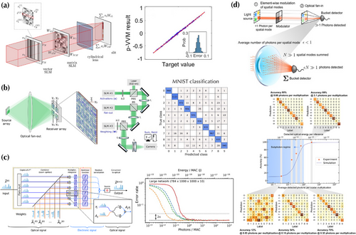
In addition, Bernstein et al. experimentally demonstrated a large-scale optical single-shot matrix-vector multiplication system and deployed it to inference deep neural networks.[31] As illustrated in Figure 3b, free-space optics can realize high-density () 3D information routing and processing in a high-throughput and energy-efficient manner. For the multiplication implementation, high-speed gigahertz-rate optical sources, such as vertical-cavity surface-emitting lasers[35] and micro-LEDs,[36] encode an input vector; free-space optical components, such as a reconfigurable diffractive optical element using a liquid-crystal-on-silicon SLM, duplicate and fan-out to optoelectronic weighting elements, which can also be implemented using a liquid-crystal-on-silicon SLM; photodetectors after the weighting SLM can perform summation operation by summing up analog current through Kirchhoff's law. Further, this matrix-vector multiplication system has been deployed in a fully connected neural network to perform an ML task of classifying the handwritten digits from the Modified National Institute of Standards and Technology (MNIST) dataset. The nonlinear activation function is introduced in electronic circuits in detectors. Figure 3b also displays the confusion matrix of MNIST classification with an accuracy of , which is comparable with the accuracy using a standard digital computer ().
Moreover, Hamerly et al. proposed a simplified system architecture to perform matrix-vector multiplications based on homodyne detection, which is fast, low power, compact, and scalable to a large number of () neurons.[32] As shown in Figure 3c, the vector elements are encoded in time steps of a time sequence and fanned out into multiple channels. Each row of matrix elements is also encoded in time steps of a time sequence and different rows are input into different channels. Suppose signals for encoding vector and matrix elements are from the same coherent source and the coherence length is long enough. In that case, the charge accumulated by the homodyne detector is proportional to the multiplication of matrix and vector elements and nonlinear functions can be implemented in electronics. The advantage of the balanced homodyne detector is its fast data processing speed and automatic multiplication performed optoelectronically.[37] The proposed optical systems are further evaluated through simulations in fully connected layers of an ML model to classify the MNIST dataset, revealing an ultralow 50 zetajoules per multiply and accumulate energy consumption determined by quantum-limited noises.
Also, Wang et al. experimentally demonstrated an energy-efficient optical dot product (i.e., vector–vector multiplication) system with a scale and sub-photon-per-multiplication, and deployed it in a deep neural network.[33] As shown in Figure 3d, vector elements are encoded into the intensity of each light source pixel and the transmittance of each SLM pixel, respectively. Dot products are computed through the element-wise multiplication of light source and SLM pixels and the optical fan-in to physically sum up the multiplication output by focusing the light onto a detector. For a specific detector with a certain shot-noise limit, a large vector size and the optical fan-in can enable less-than-1-photon-per-scalar multiplication operations with extremely low optical energy consumption. The proof-of-concept system is evaluated in a four-layer fully connected multilayer perceptron (MLP) model for classifying the MNIST dataset as a function of various numbers of photons per multiplication; see Figure 3d. The accuracy decreases with decreasing the number of photons per multiplication. Using 3.1 photons leads to a accuracy and using photons leads to a lower accuracy.
3.2 Novel Materials and Devices
Although current technologies of light sources, SLMs, and photodetector arrays are mature and scalable, they have limitations and hit the bottleneck of further improving the performance. For example, liquid-crystal-based SLMs have limitations such as low frame refresh rates (e.g., 60 Hz) due to an intrinsically slow modulation mechanism based on the movement of liquid crystal molecules and electrical addressing circuits, volatile operations, and large device footprints. Exploring new optical materials and device architectures will facilitate a technological leap toward the implementation of next-generation optical computing systems. In ref. [38], Gao et al. proposed mid-infrared SLMs and photodetector arrays for performing matrix-vector multiplications by utilizing the extraordinary optoelectronic properties of 2D graphene, such as large carrier mobility, broadband optical response, and fast electrical tunability.[43, 44] As shown in Figure 4a, each modulator unit of the SLM consists of monolayer graphene and an extraordinary optical transmission (EOT) metamaterial on top.[45-48] By adjusting the carrier concentration or Fermi level of the graphene layer through an electrical gating between the top EOT metamaterial and the bottom transparent electrode, the optical transmittance can be electrically controlled. Similarly, each detector in the detector array is a graphene photoconductive detector, also consisting of EOT metamaterials on top of a monolayer graphene. The electrically controllable Fermi level through the electrical gating and the Pauli blocking process tune graphene absorption and thus the photoresponsivity of the photoconductor. All the inner metals of EOT structures are connected to harvest currents from each pixel along the same row to implement the summation operation. The proposed devices are incorporated into a free-space optical matrix-vector multiplication system by encoding vector elements into SLM transmittance and matrix elements into detector photoresponsivity. Figure 4a shows that the system can perform accurate calculations and be utilized in various ML algorithms, including singular value decomposition, support vector machine, and deep neural networks, such as MLP models. The large carrier mobility and highly efficient electro-optic control of graphene devices lead to high data throughput and low energy consumption in performing these ML algorithms using optical systems. Moreover, Benea-Chelmus et al. experimentally demonstrated an efficient GHz SLM based on a hybrid silicon-organic metasurface platform that leverages Mie resonances in metasurfaces and the intrinsically fast electro-optic Pockels effect in high-performance organic molecules.[49] In addition to leveraging different modulation mechanisms to improve SLMs for high system throughput, another important factor is from electrical driving circuits, such as digital-analog converters (DACs). A potential approach for improvement is to construct a large array of fast DACs[50] to match SLM speed and drive each SLM pixel in parallel. Further, the electrical circuits in SLMs can be seamlessly integrated with high-speed input/output interfaces in state-of-the-art graphic processing unit architecture to fully unleash the high-throughput processing advantage in optical systems.
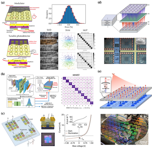
In addition, nonvolatile phase change materials (PCMs) are emerging as another promising material for optical computing systems due to the following reasons. First, the PCM states can be fast and reversibly reconfigured between crystalline and amorphous phases with an electrical or optical pulse.[51-53] Second, the PCM states can be preserved without external stimulus for years[54, 55] so that static energy consumption is minimal.[56] Third, the tunable range of optical properties is large over a wide spectral range,[51] enabling compact and broadband operations for free-space optical components and systems.[57-62] Fourth, PCMs are scalable[63] and compatible with other materials for integration. Tang et al. described a device-system end-to-end design methodology to optimize a free-space optical general matrix multiplication system by engineering an SLM made from chalcogenide PCM germanium-antimony-tellurium;[39] see Figure 4b. With a hardware simulator and experimental information, the design of each reconfigurable unit is achieved by directly optimizing system calculation accuracy using reinforcement learning algorithms, including deep Q-learning neural network, Bayesian optimization, and their hybrid approach. The algorithm-generated physical quantities show a clear correlation between system performance metrics and device specifications. Furthermore, the system is trained and deployed to multiple ML tasks, including MNIST image classification, quantum material discovery, and a closed-loop design of optical ML systems, showing good performance.
Other 2D materials, such as semiconducting transition metal dichalcogenides, are also promising to construct intelligent detector arrays because of their electrically controllable properties.[64-66] For example, Mennel et al. demonstrated an image sensor based on a reconfigurable 2D photodiode array with the weight or matrix information encoded in a continuously tunable photoresponsivity,[40] as shown in Figure 4c. Hence, this intelligent sensor array can perform a real-time multiplication of the projected optical image with a photoresponsivity matrix. The photoresponsivity matrix can be trained through supervised and unsupervised learning to simultaneously sense, classify, and encode images without latency and a throughput of 20 million bins per second.
Furthermore, advanced semiconductor manufacturing nowadays offers high-density on-chip integration of high-performance device components to improve the overall efficiency and enable new functionality of optical computing systems. For example, Chen et al. demonstrated a spatial-temporal-multiplexed optical neural network based on matrix multiplications implemented using volume-manufactured micrometer-scale-vertical-cavity surface-emitting laser (VCSEL) arrays,[67, 68] which exhibit efficient electro-optic conversion and compact footprint to address existing challenges;[41] see Figure 4d. Similar to Figure 3c, vector and matrix elements are encoded in time steps of a time sequence, which is generated by the direct modulation of each VCSEL unit. The fan-out is achieved through a diffractive optical element similar to Figure 3b. Multiplication and nonlinear operations are performed using homodyne detection (Figure 3c), allowing matrix operations at the quantum-noise limit and detection-based optical nonlinearity with instantaneous response. The system reaches an energy efficiency of seven femtojoules per operation with a compute density of six tera-operations , representing 100-fold and 20-fold improvements, respectively, over state-of-the-art digital processors. Moreover, Panuski et al. created an SLM that can have complete control of space and time degrees of freedom of optical fields through a programmable photonic crystal cavity array as illustrated in Figure 4e.[42] Specifically, a high-speed micro-LED array illuminates an array of photonic crystal cavities. The illumination induces electrical permittivity change by photoexcited free carriers,[69] leading to either phase-dominant, amplitude-dominant, or coupled amplitude–phase modulation of the transmitted light depending on the coupling condition. This free-carrier dispersion enables fast ( MHz) and low-energy (femtojoule order) modulation. In particular, this structure can be implemented using a 300 mm foundry process at large scale (Figure 4e).
3.3 Advanced Applications
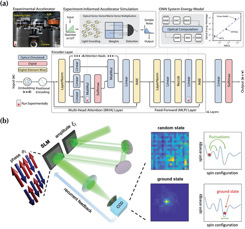
The optical multiplication systems are mainly benchmarked with respect to standard image classification tasks, such as classifying the MNIST database. However, their potential applications can be broad and beyond current demonstrations. For example, Anderson et al. showed the ability to run ML transformer models[72] on optical matrix-vector multipliers through proof-of-concept optical experiments and experiment-informed numerical simulations;[70] see Figure 5a. The scaling behavior of transformers is examined versus optical energy usage and model size, showing that optical systems have a large and asymptotic energy advantage over digital ones that grow with the model size. Under realistic assumptions, a future optical accelerator can deliver orders-of-magnitude energy consumption advantages over state-of-the-art electronic processors. Besides ML applications, matrix and vector multiplications are also ubiquitous for quantum applications. For example, various optical Ising machines have been demonstrated as fast computing systems for the Hamiltonian energy minimization of Ising models, essentially solving a combinatorial optimization problem of finding optimal spin states.[71, 73-75] The typical architecture of spatial optical Ising machines is implemented by encoding spin states and by programming Hamiltonian using SLMs through optical vector-matrix multiplications, as shown in Figure 5b. The recurrent feedback tasks the output image captured on a camera to evolve the SLM configuration to reach the Ising ground state with minimum energy.
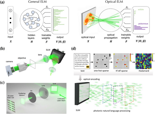
So far, the processes in optical matrix and vector multiplication systems need to be arranged to have the same mathematical function. This requirement can be relaxed in optical architectures that do not need the control of the entire network, such as extreme learning machines (ELMs). Huang et al., for the first time, proposed the ELM as a learning scheme for providing generalization performance at extremely fast learning speed using single hidden layer feed-forward neural networks.[79, 80] As shown in Figure 6a, a general ELM consists of a hidden layer with fixed connections that are not trained. Only a single out layer is trained to map the hidden layer to specific computational tasks. In optical implementations, this hidden layer can be a physical scattering or free-space propagation process. For example, Saade et al. employed a digital micromirror device to encode the input by amplitude modulation, and achieved the hidden layer by random complex projections and the elliptic kernel using lenses, a polarizer, and a multiply scattering medium consisting of a thick layer of nanoparticles.[81] Later Pierangeli et al. demonstrated another optical ELM based on free-space propagation (Figure 6b).[76] The system includes a spatial light modulator as the input encoder. The feature mapping space is achieved by far-field coherent wave propagation in free space and nonlinear detection by the saturation effect of the camera pixels. Learning has been experimentally demonstrated from data on various classification and regression tasks, achieving accuracies comparable with digital kernel machines. In addition to conventional cameras, Zhang et al. experimentally demonstrated the feasibility of using perovskite solar cells for capturing output states from the hidden layer (Figure 6c).[77] A set of just six distinct solar-cell elements is employed for completing classification tasks, showing that the solar-cell-based setup outperforms the same setup with conventional cameras of the same resolution. Furthermore, M. Valensise et al. extended the application of the optical ELM for natural language processing by encoding texts into the optical wavefront from a phase-only SLM (Figure 6d).[78] The obtained optical processor for supervised learning can achieve a capacity exceeding optical nodes, more than one order of magnitude larger than any previous implementation, which enables optical large-scale text encoding and classification.
4 Free-Space Diffractive Optical Neural Networks
As mentioned in Section 2, Fourier and inverse Fourier transformations are another two core operations that can be implemented with free-space optical systems. In principle, any linear transformations can be achieved through successive Fourier and inverse Fourier transformations. Built upon these principles and with modern hardware, DONNs have recently attracted great research interest to optically perform ML tasks through spatial light modulation and optical diffraction of coherent light in multiple diffractive layers. The DONN architecture is similar to the architecture shown in Figure 1c, but the difference is that the transparencies in DONNs are replaced with diffractive layers that diffract light. Hence, the lenses in Figure 1c are not needed anymore. The spatial light modulation on each diffractive layer regulates the amplitude and phase of the input electric field and performs element-wise multiplication. The optical diffraction between diffractive layers performs Fourier transformation based on scalar diffraction theory.[82] In this section, we will review the hardware implementation, the training, the multiplexing, the reconfigurability, and the advanced applications of DONN systems.
4.1 Implementation of DONN Systems
Lin et al. pioneered the creation of the first DONN system in the terahertz (THz) wavelength range by leveraging mature 3D printing technology.[86] Figure 7a displays an illustration and a photo of a fabricated five-layer THz DONN system illuminated by a coherent THz image. Pixels on diffractive layers have various heights to modulate the phase of transmitted light. The pixel heights in all diffractive layers are trained or optimized so that input images can converge into a pre-defined detector region, which represents the meaning of the input imaging. Note that the parameters controlling diffraction patterns, such as pixel heights in the current example and SLM driving voltages in reconfigurable DONNs as discussed later, are directly trained. There is no correspondence between diffraction patterns and weight matrices in optical matrix and vector multiplication systems. In this way, the DONN system can perform ML classification tasks. The 3D-printed THz DONN system has been demonstrated to successfully classify handwritten digits in the MNIST dataset and fashion products in the Fashion-MNIST dataset with good accuracy.
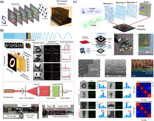
However, the practical technologies for generating, manipulating, and detecting THz waves are limited[87] and the THz DONN system requires special, costly, and complicated equipment. Thus, it becomes desirable to extend DONN systems from the THz wavelength range to visible and near-infrared ranges, where optical hardware is more accessible and compact and advanced diffractive layers, such as metasurfaces, can be employed. For example, Chen et al. constructed a visible DONN system at 632.8 nm to classify the MNIST dataset with five diffractive layers on substrates;[84] see Figure 7b. Diffractie layers are fabricated using photolithography and etching processes. The experimentally obtained accuracy is 84% and the simulation accuracy is 91.57%. Moreover, Luo et al. demonstrated a metasurface-based DONN system integrated with a complementary metal-oxide semiconductor (CMOS) imaging sensor, which can perform on-chip multichannel and multitasking imaging processing in the visible range;[85] see Figure 7c. The metasurface consists of an array of subwavelength nanopillars with the capability of arbitrarily manipulating the optical wavefront in a highly efficient manner.[88, 89] The compact metasurface leads to high-density integration of diffractive pixels with an areal density up to . In contrast, the pixel areal density in the THz DONN system is , which is orders of magnitude smaller. The metasurface can also encode information in orthogonal polarizations simultaneously, further improving the capacity of DONN systems through polarization-based multiplexing as discussed later.
4.2 Training of DONN Systems
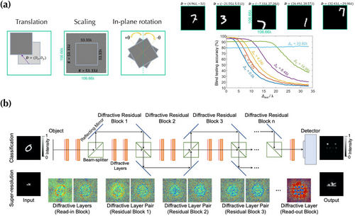
The performance of DONN systems is generally vulnerable to system imperfection and the optimization of diffractive layers (i.e., training process) is challenging when the system size, including the number of pixels in each diffractive layer and the number of diffractive layers, is large because of the gradient vanishing. Hence, the efficient and robust training of DONN systems is crucial for deploying such systems for applications. To mitigate system imperfections, such as translation, scaling, rotation, and misalignment among input images and diffractive layers, Mengu et al. quantified the sensitivity of DONN systems concerning these imperfections and developed a training strategy that incorporates these factors as random variables;[90] see Figure 8a. Hence, this training method enables the optimization of diffractive layers to be shift-, scale-, and rotation-invariant. Mengu et al. further introduced layer-to-layer misalignment as random variables in the training process to obtain robust DONN systems against misalignments, while at the cost of reduced classification accuracy.[91] Further, to mitigate the gradient vanishing problem in training large and deep DONN systems, Dou et al. introduced the residual deep neural networks consisting of diffractive residual learning blocks to directly connect the input and output between optical layers;[92] see Figure 8b. These direct paths can not only provide the capability of deep DONN systems for handling complex ML tasks but also offer direct paths for gradient backpropagation in training substantially deep networks to avoid the gradient vanishing and exploding problems during backpropagation.[93] This architecture and the spirit of training are similar to ResNet in computer vision.[94]
Still, the current training of DONN systems is performed based on electronic computer models to obtain parameters for physical implementations (i.e., in silico training). The major drawback of in silico training is the inevitable discrepancy between models and physical systems, leading to degraded performance when deploying trained models. If DONN systems contain reconfigurable diffractive layers, which will be discussed later, in-situ training approaches can be designed for efficient training and better system performance. For example, Zhou et al. demonstrated that the gradient at each diffractive layer can be calculated with measured forward and backward-propagated optical fields based on the light reciprocity and phase conjunction principles, allowing the optical backpropagation of the network residual errors by propagating the error optical field backward.[95] In the forward propagation, optical fields at each diffractive layer and output and the error field between the output and ground truth can be measured; in the backward propagation, optical fields at each diffractive layer can be measured by taking the error field at the output and propagating backward. The gradients at each diffractive layer can be calculated following backpropagation equations and then employed to update each diffractive layer. Since the gradient is calculated based on actual experimental measurements, various errors between models and physical systems have been incorporated into the training, leading to improved system performance.
4.3 Multiplexing of DONN Systems
The versatility of free-space optical systems enables the various parallel multiplexing schemes, such as path-, polarization-, and wavelength-multiplexing, in the architecture of DONN systems, which can significantly improve system performance and create new functionalities. For example, conventional detectors in DONN systems can only capture nonnegative values of light intensity at the output without phase information, somehow limiting system performance. To mitigate the detector nonnegativity, Li et al. demonstrated a differential detection scheme that employs two detectors per data class at the output and the training process is to maximize the signal difference from the detector pair;[96] see Figure 9a. The DONN system with jointly optimized separate diffractive layers for positive and negative detectors shows improved classification accuracy in MNIST, Fashion-MNIST, and grayscale CIFRA-10 datasets, when compared to the conventional DONN system of a similar size. Furthermore, Rahman et al. proposed an approach of using feature engineering and ensemble learning with multiple independently trained diffractive layers to enhance the classification accuracy of DONN systems;[97] see Figure 9b. Specifically, a set of input filters is utilized to extract features from preprocessed input images and each feature image passes through a DONN system with the differential detection scheme mentioned before. Selected output channels from multiple DONN systems form an ensemble for classification, which can achieve accuracy for the CIFAR-10 dataset as . This value is improved compared to the average performance of the individual DONNs.
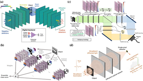
Deploying different ML tasks using the DONN systems we have discussed so far requires the reconstruction of the entire system since the spatial light modulation responses of diffractive layers are fixed once they are fabricated. This can be partially addressed through multiplexing. For instance, Li et al. described a path-multiplexing multitask learning DONN architecture shown in Figure 9c, which can automatically recognize which task is being deployed in real-time and perform corresponding classification.[98] Instead of constructing two separate DONN systems for MNIST and Fashion-MNIST datasets, a few diffractive layers can be shared and two split branches of diffractive layers are tailored for these two ML tasks. The simulation calculation results demonstrate that the multitask DONN system can achieve the same accuracy for both tasks compared to two separate DONN systems while with improvement in hardware utilization efficiency. In addition to path-multiplexing, the intrinsic physical quantities of optical waves, such as polarization, can also enable parallel processing with multiplexing. For example, the metasurfaces developed by Luo et al. can enable not only compact integrated DONN systems as shown in Figure 7c but also the polarization-multiplexing capability. The effective refractive indices of subwavelength nanopillars are different along two orthogonal polarization states, which are utilized to perform two classification tasks simultaneously for the MNIST and Fashion-MNIST datasets. Furthermore, the multiplexing can also simplify the hardware implementation of DONN systems, which is particularly critical for the technically challenging THz range. For example, instead of requiring a detector array for different classes, Li et al. demonstrated a broadband wavelength-multiplexing THz DONN system that assigns each image class in the MNIST dataset to different wavelengths;[99] see Figure 9d. Thus, only a single-pixel detector is needed at the output end.
4.4 Reconfigurability of DONN Systems
Although multiplexing can help to perform a few limited tasks in the same DONN system, it is more desirable to be able to fully dynamically adjust the response of diffractive layers for reconfigurable DONN systems. The central component for such implementation is an SLM, in which the modulation of the amplitude and phase of transmitted or reflected light can be controlled with electrical signals. Zhou et al. have made a major advance in implementing a large-scale reconfigurable DONN system by replacing non-reconfigurable diffractive layers with an electrically-controllable liquid-crystal SLM.[100] Specifically, the system is built upon a fundamental reconfigurable diffractive processing unit (DPU) containing a DMD, a phase-only SLM, and a CMOS detector, as shown in Figure 10a. The DMD encodes input images; the SLM is a reconfigurable diffractive layer; and the CMOS reads out the output image and converts it to electrical signals. Through the connection of the sensor in one DPU and the DMD in another DPU, many DPU blocks can be cascaded to construct nearly arbitrary neural network architectures including DONNs and diffractive recurrent neural networks for complex ML tasks. However, there are still electrical-to-optical (E/O) and optical-to-electrical (O/E) conversions between layers. These conversions lead to increased energy consumption and processing latency, and the discrepancy between models and physical systems, limiting the reconfigurability.
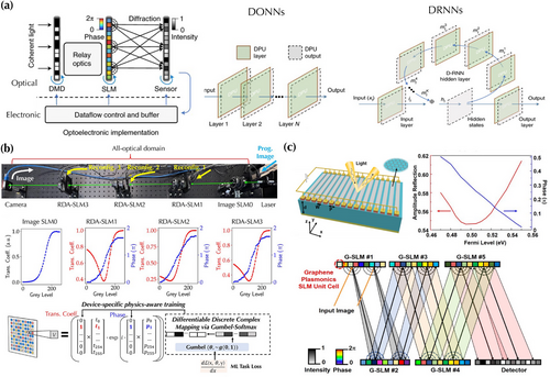
Instead, Chen et al. developed an all-optical fully reconfigurable DONN system utilizing directly cascaded liquid-crystal SLMs in the visible wavelength range without interlayer E/O and O/E conversions;[101] see Figure 10b. The experimentally measured modulation response of each SLM displays a coupled amplitude and phase modulation under discrete excitation voltages, which breaks down the traditional backpropagation of gradients. In order to enable differentiation with discrete device responses, a device-specific physics-aware training approach is developed by employing the categorical reparameterization with Gumbel-Softmax for arbitrary device responses.[103] In addition, the diffraction model is modified from standard scalar diffraction theory to a system-specific convolutional Fresnel method.[104] Further, the full system reconfigurability enables fast and precise pixel-by-pixel optical alignment. Hence, such a full-stack implementation of software and hardware guarantees that in-silico-trained models can be accurately deployed to the physical system without further adaptive tuning, which has been confirmed in ML tasks of classifying MNIST and Fashion-MNIST datasets.
However, technology to achieve reconfigurable SLMs is not always on the table like the liquid crystal technology for visible light. For example, in the THz wavelength range, there is no reconfigurability in current THz DONN systems. The conventional design wisdom assumes that a stringent specification of a full-range phase-only modulation is needed for SLMs, posing a great challenge for practical implementations. In contrast, Zeng et al. proposed an active reflective graphene-plasmonics-based SLM for reconfigurable THz DONN systems;[102] see Figure 10c. By coupling the plasmonic resonance in graphene nanoribbons with the reflected Fabry-Pérot mode from a back reflector, a substantial /2 phase modulation with minor amplitude modulation of the reflected light can be achieved. Moreover, the DONN system built from the arrays of designed SLM can achieve classification accuracy of the MNIST dataset, which is comparable to similar systems built from components with a phase range. This relaxes the SLM requirement from a phase-only modulation to a coupled amplitude-phase modulation with a phase modulation range, significantly simplifying and enabling varieties of SLM designs for reconfigurable THz DONN systems.
4.5 Novel Applications of DONN Systems
The demonstrated and benchmark applications of DONN systems are mainly image classification tasks, such as recognizing images in the MNIST and Fashion-MNIST datasets, limiting the prospect of developing and utilizing such hardware. To expand the horizon of DONN system applications, Chen et al. pioneered creating a universal feature engineering approach to convert any categorical input features to images, which can be processed in the reconfigurable DONN system to obtain categorical output;[105] see Figure 11a. Through this approach, the reconfigurable DONN system has been experimentally deployed in a broad range of scientific computing domains, including guiding 2D quantum material synthesis, predicting the properties of 2D quantum materials and small molecular cancer drugs, predicting the device response of nanopatterned integrated photonic power splitters, and the dynamic stabilization of an inverted pendulum with reinforcement learning. Similarly, Qian et al. demonstrated that the DONN system can also be used for performing optical logic operations by spatially encoding the incident plane wave following logic operations at the input layer;[106] see Figure 11b. The diffractive layers consist of metasurfaces and are trained to have the diffractive light to focus on the desired logic output.
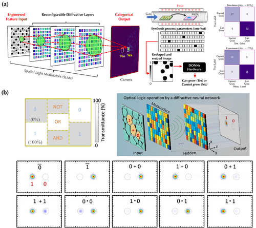
Moreover, very recently, Tang et al. demonstrated an optical neural engine architecture combining DONN systems for Fourier space processing and optical matrix-vector multiplication systems for real space processing to solve time-dependent and time-independent partial differential equations (PDEs) in diverse disciplines, including Darcy flow equation, the magnetostatic Poisson's equation in demagnetization, the Navier-Stokes equation in an incompressible fluid, Maxwell's equations in nanophotonic metasurfaces, and coupled PDEs in a multiphysics system.[107] This architecture offers a versatile and powerful platform for large-scale scientific and engineering computations.
5 Conclusion
This review has described the pioneering early works and current development of two 3D free-space optical computing systems, matrix, and vector multiplication systems and DONN systems. We have covered hardware implementations of such systems from material, device, and system architecture perspectives. In addition, we have discussed the deployment of these systems for various applications. The major challenge associated with free-space optical computing systems is still their large system footprint. We envision that the hybrid integration of integrated high-density SLM and photodetector array circuits for information processing and engineered metamaterials and photonic crystals for compact free-space information routing[108] can combine advantages and mitigate disadvantages of 2D and 3D optical systems.
Acknowledgements
R. C. and W. G. acknowledged the support from the National Science Foundation through Grants No. 2316627 and 2428520.
Conflict of Interest
The authors declare no conflict of interest.
Biographies

Ruiyang Chen is a fifth-year Ph.D. student in the Department of Electrical and Computer Engineering at the University of Utah. Before coming to Utah, he received his M.S. degree in Electrical and Computer Engineering from the University of Notre Dame and his B.S. degree in Physics from the University of Science and Technology of China. His research focuses on reconfigurable photonics for optical machine learning.

Dr. Weilu Gao is an Assistant Professor in the Department of Electrical and Computer Engineering at the University of Utah, United States. He received his B.S. degree in electrical engineering from Shanghai Jiao Tong University in 2011 and his Ph.D. degree in electrical and computer engineering from Rice University in 2016. His research interests are in photonic and optoelectronic materials, devices, and systems, especially the hardware and software development for optical computing architectures.


